The particular strength lies in the development of smart integrated systems for different applications. With our partner Fraunhofer ENAS, we develop single components, technologies for their manufacturing as well as system concepts and system integration technologies and transfers them into production. The institute offers research and development services from the idea, via design and technology development or realization based on established technologies up to tested prototypes.
Advanced Nanosystems and Microelectronics
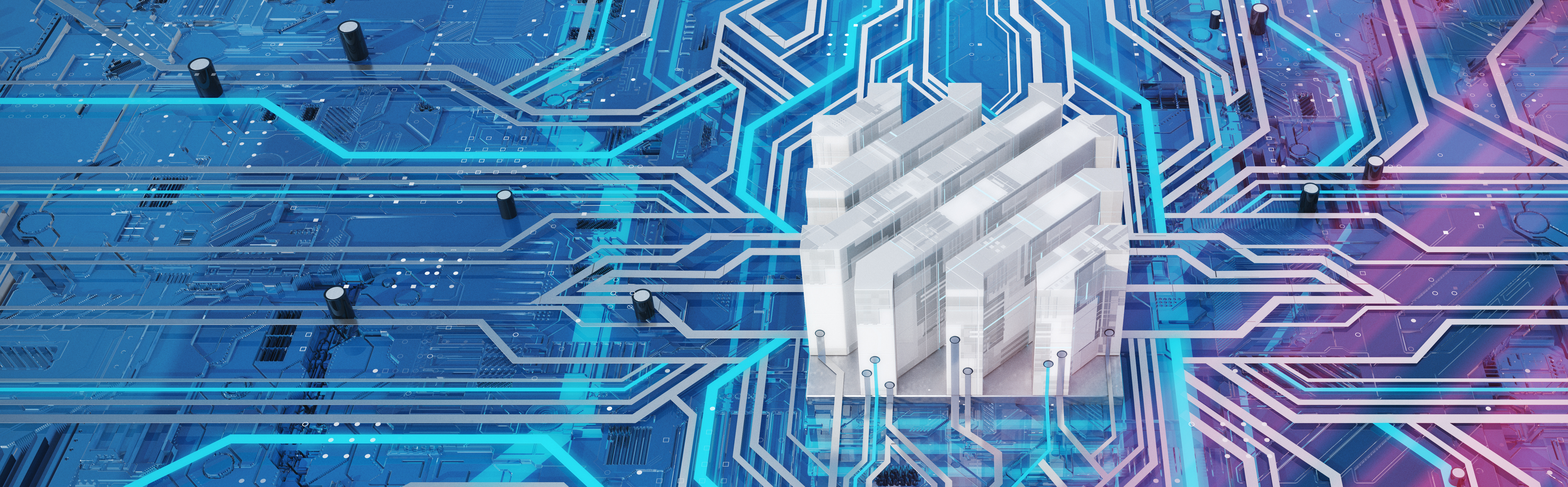
Innovation portfolio in cutting-edge research at the intersection of nanotechnology and electronic systems transforming the future of technology.
Advanced Nanosystems and Microelectronics
Research and Competence Areas
The particular strength lies in the development of smart integrated systems for different applications. With our partner Fraunhofer ENAS, we develop single components, technologies for their manufacturing as well as system concepts and system integration technologies and transfers them into production. The institute offers research and development services from the idea, via design and technology development or realization based on established technologies up to tested prototypes.
Beyond CMOS and RF devices, integrated circuits and technologies
At Fraunhofer, we excel in the development of cutting-edge technologies and devices that go beyond traditional CMOS and RF devices. Our competencies lie in the advancement of memristive devices and circuits, particularly for applications in neuromorphic and in-memory computing. Through extensive research and innovation, we are actively contributing to the realization of efficient and powerful computing systems that mimic the human brain's neural networks. Additionally, we specialize in the development of technology, devices, and circuits based on Carbon Nanotubes (CNT-FETs). Our focus in this domain revolves around analog high-frequency applications and hardware security. By harnessing the unique properties of Carbon Nanotubes, we strive to create advanced solutions that address the ever-evolving demands of the modern technological landscape.
Packaging and (heterogeneous) integration (2D, 2.5D, 3D) for electronic devices.
We are at the forefront of packaging and heterogeneous integration research. Our expertise lies in the development of processes that enable seamless integration of electronic devices, particularly focusing on wafer-level packaging. We specialize in various aspects of the integration process, including joining and contacting processes, thin film encapsulation, and screen printing for metallization and soldering. By pushing the boundaries of packaging technologies, we enable the realization of advanced electronic devices that are compact, reliable, and highly efficient. Our commitment to innovation and collaboration ensures that we remain at the forefront of packaging and integration advancements, supporting the needs of diverse industries.
Process and device modelling and simulation
We specialize in the development of knowledge-enhanced process models that utilize artificial intelligence and physical methodologies. Our expertise covers a wide range of semiconductor processes and metrology, both in the front-end and back-end stages. By leveraging advanced modeling and simulation techniques, we provide invaluable insights into process optimization, performance prediction, and yield enhancement. Additionally, our research focuses on the development of physical models for the design of beyond CMOS devices. Through the integration of innovative modeling approaches, we enable the design and realization of novel semiconductor devices that push the boundaries of conventional technologies.
Systems and Applications
We consistently follow the value creation in the research and development process and is therefore a systematic consequence of the strategic orientation. We approach the multifaceted issues of our public and industrial partners by stringently extracting the possible, meaningful and sustainable applications from the problem space and transferring them to the solution space by means of the expertise and technology available at the institute in all business areas.
In this way, it is our essential task to generate projects together with our partners - on the basis of usable applications - which support and advance the mature development of laboratory demonstrators via functional models right through to the production process of our industrial customers.
Conversely, we also provide the groundbreaking impulses for the fundamental technology developments by deriving relevant research needs of the future from the emerging applications in the industrial and public environment.